Transistor Prices Stagnate: 28nm’s 10-Year Flatline Indicates Potential Cost Increase for Newer Chips
Almost everyone knows the challenges faced by the latest process nodes, ranging from logic and memory scaling down to cost-effectiveness. Recent data indicates that transistor production costs were at their lowest almost a decade ago. Since then, we’ve tackled the ever-growing elephant in the room, increasing transistor costs.
Google Data Indicates Transistor Costs Are Expected to Increase
As highlighted by Tom’s Hardware, Zvi Or-Bach of MonolithicIC 3D reported back in 2014 that transistor prices have remained static since 28nm. For more context, the trend of cheaper transistors with each new generation was almost certain, as has been seen from 90nm–65nm, 65nm–45/40nm, and so on.
This trend unexpectedly came to a halt when TSMC introduced its 28nm process technology. While we won’t get into the specifics of why, we’re currently witnessing an uptick in the cost per transistor, which could lead to even more expensive chips.
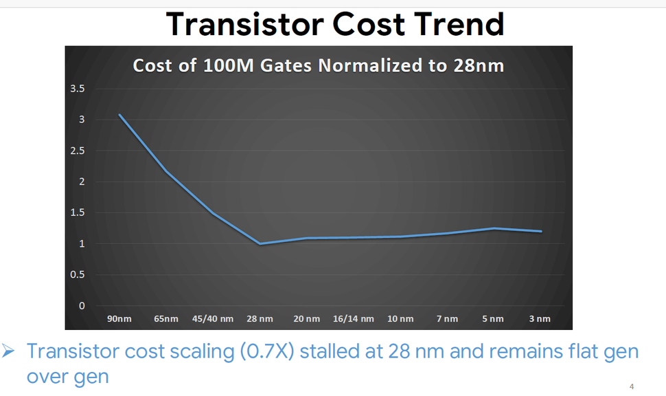
“Transistor cost scaling (0.7X) stalled at 28 nm and remains flat gen over gen”
Bleeding edge nodes, based on EUV tech require such machines from ASML. For reference, a recent shipment from ASML to Intel featured high-NA EUV scanners ranging between $300 to $400 Million.
Density improvements aren’t as drastic as well. Pat Gelsinger, CEO of Intel has finally accepted that Moore’s Law is slowing down to a 3-year cadence. In simple terms, newer transistors are complex, expensive and are require innovative methods of packaging and stacking to result in palpable improvements.
The Angstrom Era
Why move forward then? Because we can and must. Larger die sizes are first, difficult in terms of expenditure, may yield mass defects, and are less efficient than if we were to use a smaller node to scale the chip down. Since the quest for performance never stops, these giants must deliver performant yet efficient packages.
So, how do we manage this daunting task? Intel and AMD have both adopted a 3D chiplet architecture, wherein the GPU/CPU’s different components are split up, physically. Using fancy packaging such as CoWoS or Foveros, these components are built using different nodes, to optimize costs and are placed on a single package.
The shift towards the 3D Era seems inevitable and is a matter of ‘Now or Never‘, read our editorial for more insight. We also have several other technologies such as RibbonFET (GAA equivalent) and PowerVia from Intel. AMD on the contrary has a practical implementation of 3D Stacking in its X3D processors.
Source: Tom’s Hardware, Semiconductor Digest, Google