Why 3D Packaging Holds the Key to the Future of High-Speed Computing
 Reviewed by Huzaifa Haroon
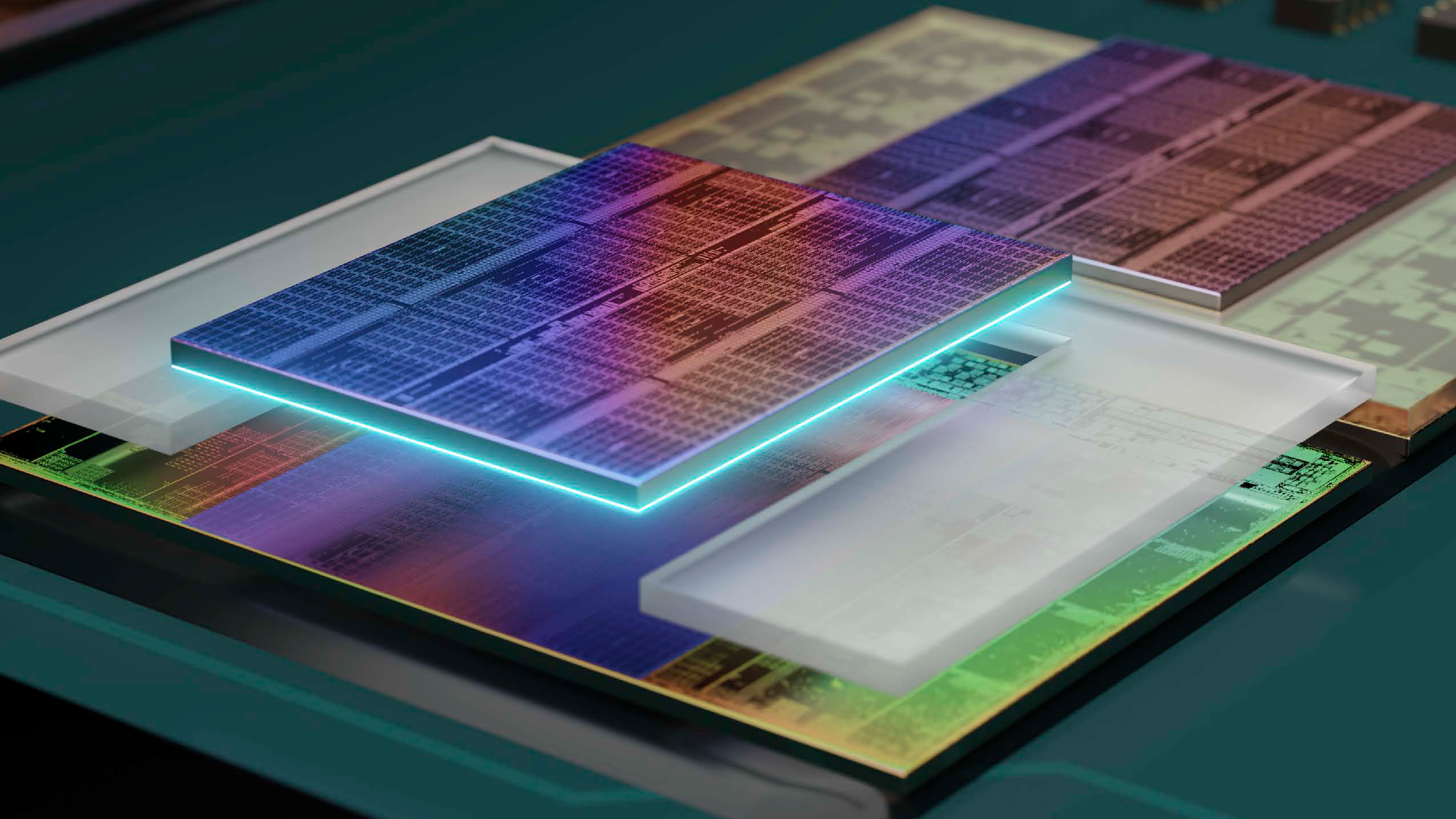
We all have heard, ‘Moore’s Law Is Dead‘ time and time again. While the actual concept behind this ‘law’ is slowing down, the generational increases are still somewhat consistent. Chip makers are experimenting with all sorts of techniques to bypass the physical limitations and financial strain of opting for a newer process node. Meet 3D chiplet packaging.
The Chiplet Approach
It goes without saying that each process node is more expensive than the last. Take TSMC for example. A 7nm-based wafer from TSMC would cost you around $10,000. Now moving over to 3nm, the same node is expected to be priced at $20,000. You can get the gist of things from here. So the question remains, “How will we get faster CPUs and GPUs in the future?”.
AMD tackled this problem by introducing chiplets. Chiplets help to reduce cost significantly. Say, you have your main Compute tile and the Input/Output tile. Manufacturing both of them at a bleeding-edge node (3nm) in a monolithic package is possible, but also an expensive solution.
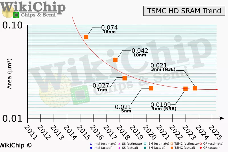
The alternative is a Multi Chiplet Module (MCM) design. What if we build our I/O die using a less expensive node, say 6nm? The I/O die probably does not need that much horsepower. The same can be said for SRAM (Cache) which is now scaling much slower than Logic. In the diagram below, 3nm is around 5% smaller in size as compared to 5nm, but costs 25% more. That is one hefty price to pay for a small increase.
Chiplets do have a few drawbacks, one of them being a slightly higher power draw and reduced efficiency. We did see RDNA3 suffer from the same issue, but nonetheless, it is cheaper to produce which in turn is better for the consumer.
Meet 2.5D and 3D IC Stacking Tech
Before we start using all those semiconductor industry buzzwords, let us actually somewhat define them.
- Die: A die is a piece of semiconductor (Silicon) on which electrical circuitry is fabricated.
- Interposer: A passive piece of silicon (mostly) that is used to connect multiple (even a single) die(s) to the package substrate.
- 2.5D Stacking: A packaging technique in which a passive interposer hosts multiple dies, side by side with one another.
- 3D Stacking: A packaging technique in which active dies are connected with one another.
Most tech experts will probably want to add more to those definitions, but we’re keeping things simple here. The headline, ladies and gentlemen is;
3D Stacking is the future.
Understanding 2.5D
Below is a sample 2.5D IC package. Basically, these small 28nm FPGA Slices are your tiles/chiplets, stacked on top of a package substrate (in green). But that’s not all. Between these two layers, lies an interposer (grey-ish). This interposer does nothing but route the electrical signals or in technical terms, it is passive.
Zoom in just a bit and you’ll see that the 28nm-based FPGA Slices are connected to the interposer by small micro bumps. The size of these bumps is called bump pitch. This is an important metric, as it can vastly increase bandwidth interconnection and the I/O density.
TSVs or Through-Silicon-Vias are vertical electrical connections that are used for silicon-to-silicon communication. This term is widely used in 2.5D and 3D stacking tech, so keep it in mind.

Understanding 3D
3D stacking is similar to 2.5D, yet it is so much different at the same time. Take it like this, in 2.5D stacking, we use a passive interposer right? Passive means it only routes electrical current. In 3D stacking, like Intel’s Foveros, the interposer is active (instead of passive), meaning that it also acts as an Integrated Circuit. Consider it like a die, similar to the compute tile (chip) placed on top of it.
3D is used for die-to-die interconnects. Similar dies are stacked on top of one another and there is no ‘passive’ interposer. 2.5D uses an interposer to connect these dies, 3D does not.
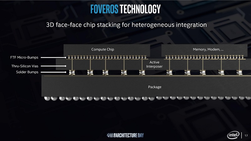
One last thing before we move on. In 2.5D, chiplets (mostly HBM) can be stacked, but they would still use an interposer. In 3D, however, there is no ‘passive’ interposer and dies are connected directly.
Problems of 3D Packaging
To keep Moore’s Law alive, we have to pay special focus to the packaging techniques we used. As explained above, 2.5D and 3D are the future. We currently do not have a ‘3D’ mainstream chip from neither AMD nor Intel. The best we currently have is 2.5D, which was introduced by AMD’s chiplet approach.
Remember the term bump pitch? Only those packaging techniques are considered ‘advanced’ that have a bump pitch size less than 100 micrometers. A smaller size, leads to higher bandwidth and higher I/O density.
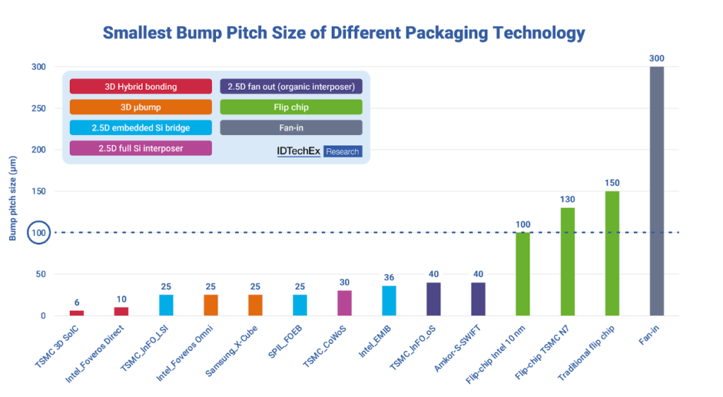
When we talk about 2.5D, the bump pitch varies from 25 µm and 40 µm (1µ = 1 micrometer). That is doable. But on moving to 3D, we are talking about bump pitch sizes in the single digits. TSMC claims that the necessary bump pitch for stacking N7 and N6 (3D) are 9 µm.
IDTechEx reports that this size will decrease to 4.5 µm for TSMC’s N3 node. This in itself is a problem. Then we have the obvious overheating complications and whatnot.
Why Does 3D Packaging Matter
Well, the question should be, “Why doesn’t it matter?“. The demand for high-speed computing is increasing day after day and we’ve barely scraped the surface. In the HPC world, companies are trying to develop revolutionary methods to decrease power consumption and increase computational throughput.
IDTechEx explains that the underlying factor that determines the growth in almost every industry is advanced packaging techniques. 5G data transmission is prone to transmission loss. This can be alleviated by bringing the antenna a tad bit closer to the RF IC or Radio Frequency Integrated Circuit.
Smartphones and smartwatches require chips that are compact and fast at the same time. This calls for some unique packaging methods, including the use of organic materials.
AMD says that, in the best-case scenario, it would require at least 500MW (1000MW = 1 Nuclear Power Plant) of power to break the ZettaFLOP barrier.
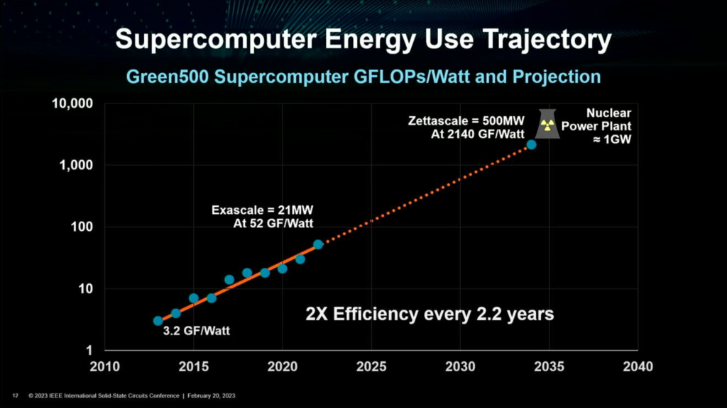
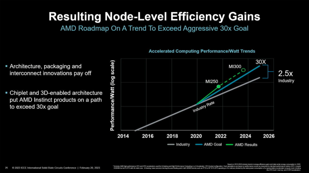
A Chiplet-powered 3D packaging approach will enable to surpass the industry’s best by a factor of 2.5x. All thanks to the efficiency offered by 3D technology. An optimized node, a faster architecture and the 3D chiplet approach may require just 100MW of power to attain 1 ZettaFLOP of performance.
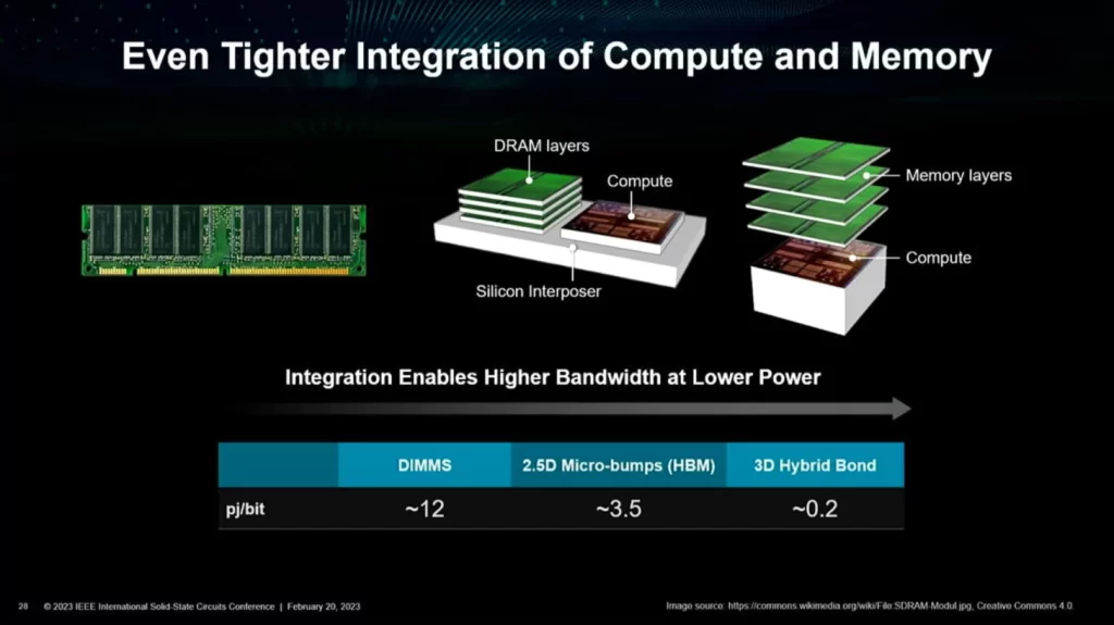
The first image is your typical DIMM configuration. The second is a 2.5D packaging technique and the last is a 3D stacked design. DIMMs use 60x more energy per bit than a 3D approach. That is simply insane, and should be more than enough to show why vertical stacking is the future and why 3D packaging matters.
Conclusion
All things considered, it is vital that engineers put their efforts and hard work in developing a new future for computing. Moore’s Law still lives strong all thanks to these innovative and state-of-the-art designs. The road ahead is rough but significant work has been done by the likes of Intel, TSMC and AMD to pave way for this major paradigm shift.
Reviewed by Huzaifa Haroon