Making An Electronic Letter Box Circuit
A letterbox is used to receive the mail sent by the sender and it is installed outside the houses or offices. The postman drops the mail into that box and later that mail is picked up the residents of the house. When the postman arrives at the house he just drops the letter into the box and goes away without apprising the residents to take that letter out. How good it would be if we automate this process so that whenever the letter is dropped into the box the residents become to know and fetch it without any delay? In this project, I will make an electronic letter box circuit that can be used in the homes as well as offices. The most vital component in this project is the LED. With technology advancement, Light Emitting Diodes (LEDs) were invented and they produced less carbon and hence, contributed to minimizing global warming. The demand for LEDs is increasing rapidly nowadays because they are not much costly and they last longer. As soon as the letter is dropped in the box the LED stops glowing and it is the sign of a letter in the box. This circuit will be placed in the letterbox that is installed outside the house and while placing the circuit special care is needed so that the letter is detected correctly. Let’s not waste a second and get this done.
How To Integrate Basic Circuit Components In The Circuit Design?
The best approach to start any project is to make a list of components and going through a brief study of these components because no one will want to stick in the middle of a project just because of a missing component. The Printed Circuit Board is preferred for assembling the circuit on hardware because if we assemble the components on breadboard they may detach from it and the circuit will become short hence, PCB is preferred.
Step 1: Components Needed (Hardware)
- No products found.
- CD4001 NOR Gate
- 1k Resistor (x2)
- 10k Resistor (x5)
- No products found.
- Light Dependant Resistor
- 0.1uF Ceramic Capacitor (x2)
- 9V Battery
- No products found.
- No products found.
- FeCl3
- No products found.
- Printed Circuit Board
- Hot Glue Gun
- No products found.
Step 2: Components Needed (Software)
- Proteus 8 Professional (Can be downloaded from Here)
After downloading the Proteus 8 Professional, design the circuit on it. I have included software simulations here so that it may be convenient for beginners to design the circuit and make appropriate connections on the hardware.
Step 3: Understanding The Working Principle
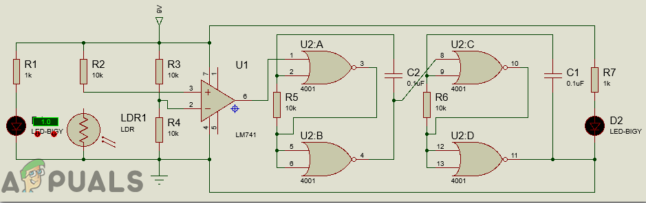
The working principle of the project is quite simple. The circuit is powered by a 9V DC battery. However, an AC to DC adapter can also be used to power this circuit because our requirement is 9V DC. We need to identify the presence of the letter in the letterbox and for identifying the letter the LDR is connected along with LED that will act as a source of light in the box. The resistance of the LDR is inversely proportional to the intensity of light which means greater the intensity of light, lower the resistance of LDR. When there is no light the resistance of LDR is very HIGH and when as soon as the light starts falling on the LDR the resistance of LDR decreases. The position of the LED is adjusted in such a way that when the light emitted by the LED directly falls on the LDR and the letter that is dropped is a box obstructs the light from falling on LDR. This change is detected by LM741 and the NOR Gate CD4001 and the LED is used to indicate the presence of a letter.
Step 4: Analysing The Circuit
The Light Dependent Resistor plays a vital role in the circuit. It is responsible for turning ON and OFF the LED. The LDR follows the principle of photo-conductivity. The resistance of the LDR varies when light falls on it. When the light falls on LDR it’s resistance decreases and when it is placed in the dark it’s resistance increases. Hence, the switching of the LED depends on the resistance of the LDR. Before reading this article it is highly recommended to read the table of logic gates of NOR. It can be googled or found Here. The Operational Amplifier 741, NOR Gate CD4001 and LDR are the backbones of the circuit. The LDR and the LED will be installed at the opening of the letter-box so that the light from the LED keeps on falling on the LDR. Hence, the OpAmp 741 will be HIGH. That signal is provided to the Pin1 of CD4001 and this NOR Gate produces the HIGH output when all of the inputs are low. Hence, the LED keeps on glowing when there is no letter in the letter-box. As soon as the letter is dropped in the box the resistance of LDR becomes very HIGH and the output of LM741 becomes LOW. This LOW signal is further provided to CD4001 that will result in (0) output at pin 3 of NOR Gate. This will generate the HIGH (1) on pin4. This is due to the inputs that are given to the second gate from pin 3 and it can be seen below in the circuit that both inputs are (0) hence the output at pin 4 will be HIGH. Due to all of the operations happening above the output at pin 11 will be HIGH and the LED stops glowing and it will indicate that there is a letter in the box. The LED stays OFF until the letters are taken out of the box and LED starts glowing again.
Step 5: Simulating The Circuit
Before making the circuit it is better to simulate and examine all the readings on a software. The software we are going to use is the Proteus Design Suite. Proteus is a software on which electronic circuits are simulated.
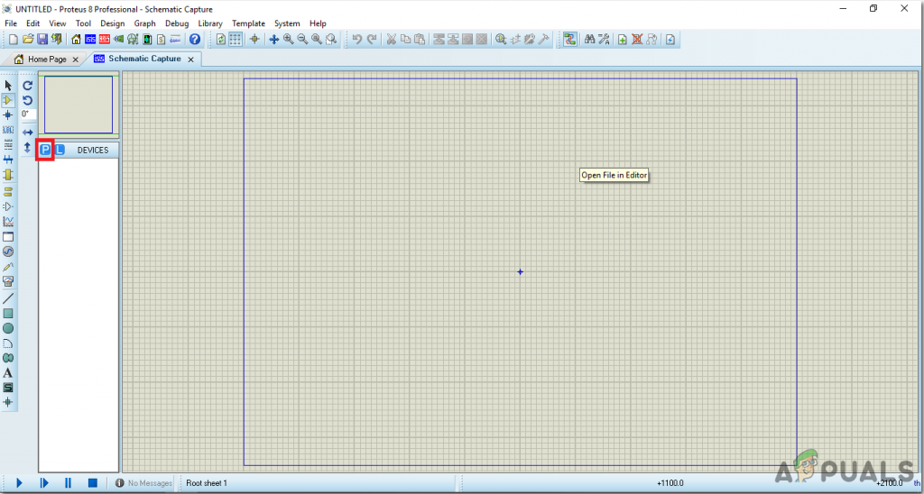
- After you download and install the Proteus software, open it. Open a new schematic by clicking the ISIS icon on the menu.

ISIS - When the new schematic appears, click on the P icon on the side menu. This will open a box in which you can select all the components that will be used.
New Schematic - Now type the name of the components that will be used to make the circuit. The component will appear in a list on the right side.
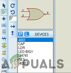
Component List - In the same way, as above, search all the components. They will appear in the Devices List.
Step 6: Making a PCB Layout
As we are going to make the hardware circuit on a PCB, We need to make a PCB layout for this circuit first.
- To make the PCB layout on Proteus, we first need to assign the PCB packages to every component on the schematic. to assign packages, right mouse clicks on the component you want to assign the package and select Packaging Tool.
- Click on the ARIES option on the top menu to open a PCB schematic.
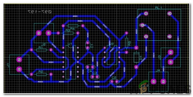
ARIES Design - From the Components List, Place all the components on the screen in a design you want your circuit to look like.
- Click on the track mode and connect all the pins that the software is telling you to connect by pointing an arrow.
Step 7: Circuit Diagram
After making the PCB layout the circuit diagram will look like this:
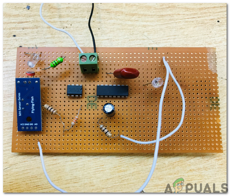
Step 8: Setting Up The Hardware
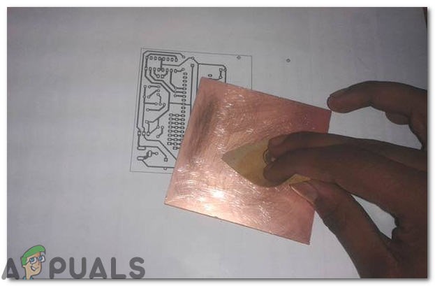
As we have now simulated the circuit on software and it is working perfectly fine. Now let us move ahead and place the components on PCB. After the circuit is simulated on the software, and its PCB layout is made, the circuit layout is printed on a butter paper. Before placing the butter paper on the PCB board use the PCB scrapper to rub the board so that the copper layer on board is diminished from top of the board.
Then the butter paper is placed on the PCB board and ironed until the circuit is printed on the board (It takes approximately five minutes).

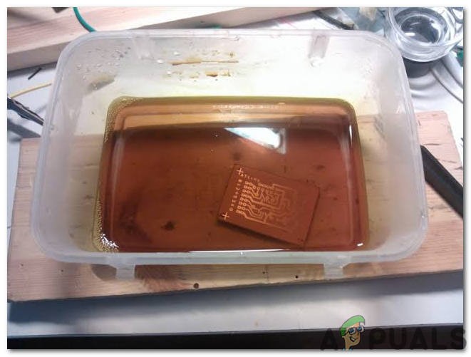
Now, when the circuit is printed on the board, it is dipped into the FeCl3 solution of hot water to remove extra copper from the board, only the copper under the printed circuit will be left behind.
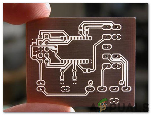
After that rub the PCB board with the scrapper so the wiring will be prominent. Now drill the holes in the respective places and place the components on the circuit board.
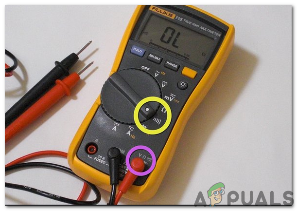
Solder the components on the board. Finally, check the continuity of the circuit and if discontinuity occurs at any place de-solder the components and connect them again. In electronics, the continuity test is the checking of an electric circuit to check whether current flow in the desired path (that it is in certainty a total circuit). A continuity test is performed by setting a little voltage (wired in arrangement with a LED or commotion creating part, for example, a piezoelectric speaker) over the picked way. If the continuity test passes, it means that the circuit is adequately made as desired. It is now ready to be tested. It is better to apply hot glue using a hot glue gun on the positive and negative terminals of battery so that the terminals of the battery may not be detached from the circuit.
Step 9: Testing The Circuit
After assembling the hardware components on the PCB board and checking the continuity we need to check whether our circuit is working properly or not we will test our circuit. Install the circuit in the letter-box that is placed outside the home and keep on monitoring the battery. When the life of the battery is finished it is replaced by the new one. This circuit can also be installed in offices.