Intel Shows Off Intel 3, 20A, 18A, Glass & Quantum Wafers at the Innovation Event
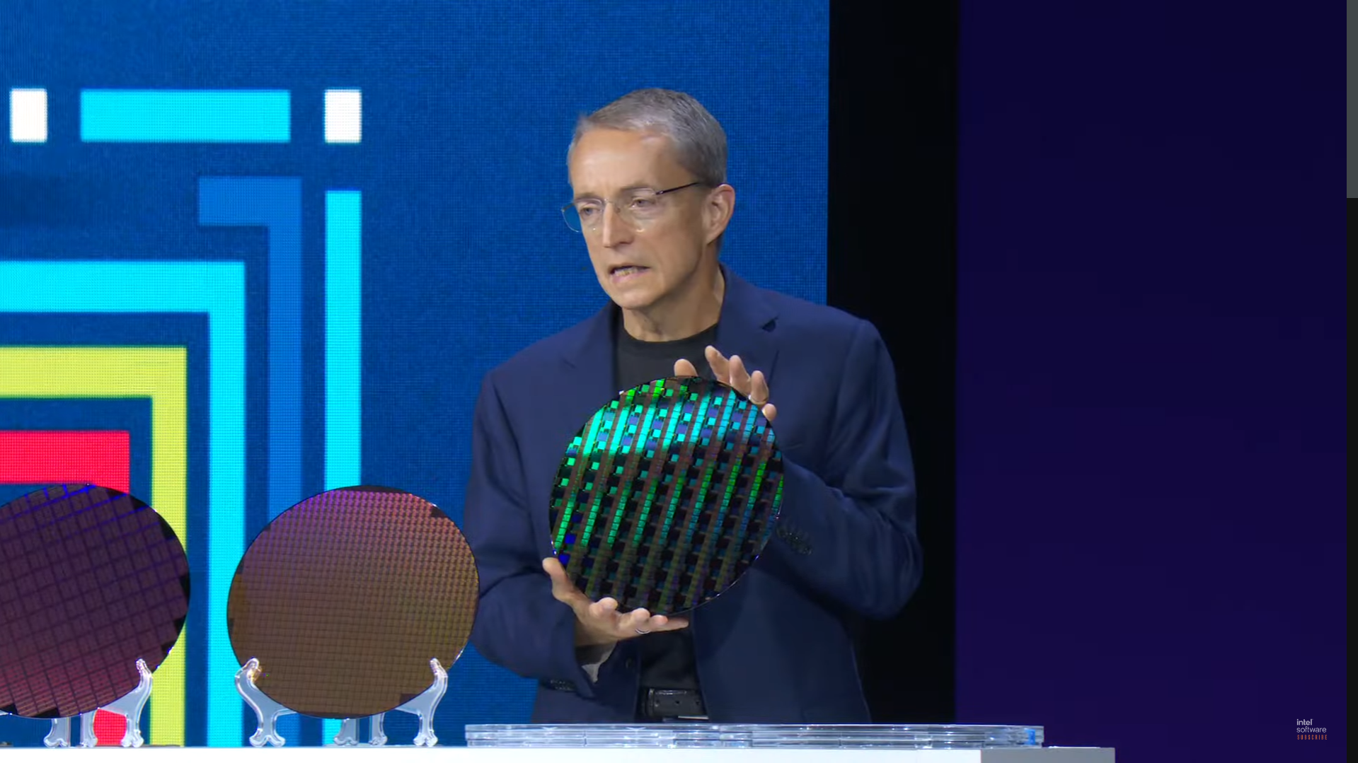
The Innovation Event is currently underway and Pat Gelsinger has displayed myraids of upcoming Intel products (and a lot of wafers). For more insight on Meteor Lake, read our detailed article on that here.
We initially expected this to be a small reveal of Meteor Lake and Raptor Lake Refresh. However, Intel has stepped things by and brought to light so many new products and wafers, that we cannot neglect their importance.
Intel 3, 20A & 18A Wafers Smile for the Camera
For the unaware, Meteor Lake is fabricated using Intel’s latest 4nm-class ‘Intel 4‘ node. Future Xeons will make use of Intel 3. As we go up the stack, Intel 20A (2nm) is planned for Arrow Lake launching next year. Moreover, we also got to see a glimpse of 18A, powering Panther Lake, scheduled for 2025.
Intel 3, used by Granite Rapids and Sierra Forest was displayed in its wafer form. Pat Gelsinger, CEO Intel, claims that Granite Rapids can offer 2.4x more efficiency than the current-gen Xeons. Granite Rapids is tipped to ship with 132 P-Cores, split across 3 dies.
Furthermore, Sierra Forest will arrive in 96-core, 128-core and 144-core flavors. With two dies fused on a single package, Intel has formed a 288-core SKU as well. This product will give some serious competition to AMD’s Bergamo which uses Zen4C efficiency cores.
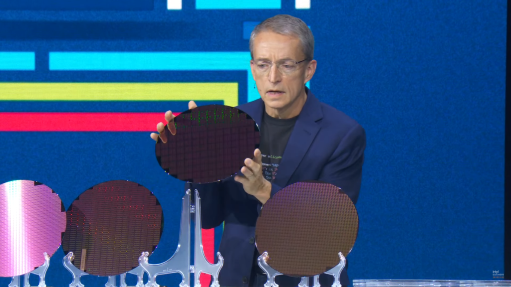
‘Intel 20A‘, the company’s 2nm-equivalent node was also showcased. This process node is reserved for Arrow Lake which is inbound next year.
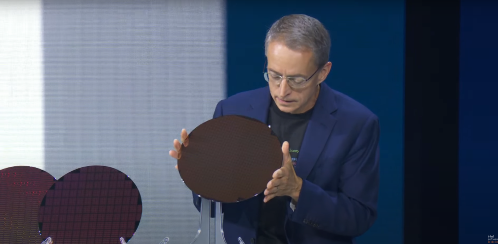
Last but not least, we set our eyes on a true beauty, Intel’s very own 18A process (1.8nm). This is merely a test chip and is unable for use in any product, for now. 18A is slated to arrive in 2025 with Panther Lake.

Panther Lake in 2025
The giant officially disclosed that Panther Lake will launch after the mobile-only Lunar Lake in 2025. Importantly, Panther Lake, as stated above is designed using the 18A process. We are not sure if Panther Lake is planned for both desktop and mobile, but Intel should confirm that as we inch closer to its launch.

Glass & Quantum Wafers
Showcasing Intel’s latest developments and breakthroughs ins the packaging field, Pat displayed a few very interesting wafers. 25 years ago, Intel defined the basis of our modern-day package, using an organic substrate.
Below is a Glass Wafer, one that Intel unveiled just yesterday. Glass wafers offer a plethora of advantages over traditional organic packages. This is the result of a decade’s worth of research and glass packaging is en route for 2030.
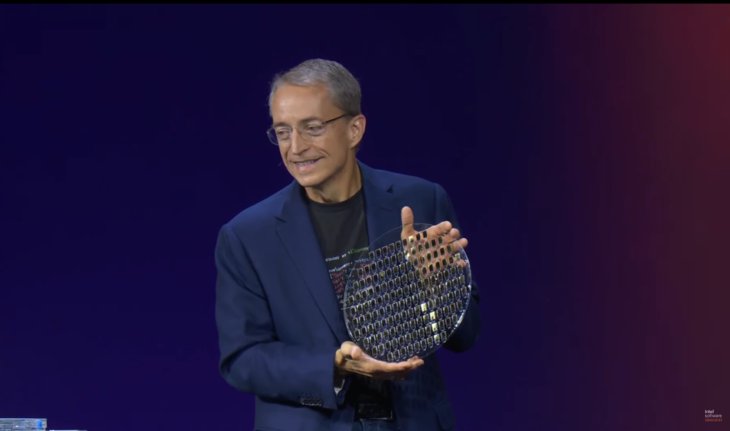
Next-up, we have a 12 Qubit wafer that powers Intel’s ‘Tunnel Falls‘ quantum products. Intel has achieved a remarkably high 95% yield rate. Due to the small size of these devices, coming in at just 50nm x 50nm, they are ~1 Million times smaller than your average chip.
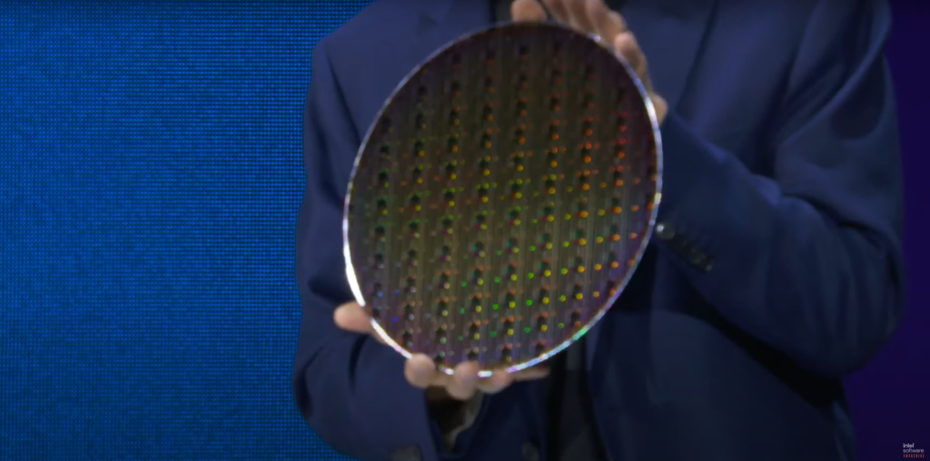
Moreover, these chips operate between 1 and 0 Kelvin (-273* Celsius). It will take Intel some serious cryogenic wizardry to get these chips to work, but the concept is enticing.
Conclusion
Despite many setbacks, Intel is keen on delivering its promise of 5 nodes in 4 years. The company’s announcements today were extremely exciting, though a bit unexpected. Likewise, Team Blue is now following a 1-year cadence between its CPU architectures, and even nodes in some cases.
Between 2023–25, the company will see a shift from Intel 7 (7nm) to Intel 18A (1.8nm). Which future Intel products are you the most excited about? Tell us in the comments below.

