Intel Details Meteor Lake: 1st Gen Core Ultra, New Performance & Efficiency Cores, Xe-LPG iGPU, Launches December 14
Intel has formally detailed its forthcoming major architecture, Meteor Lake, at the Innovation Event. Meteor Lake has historic importance for Intel as a company, paving way for the giant’s future generations.
Meteor Lake will launch on the 14th of December, alongside Emerald Rapids. Let’s talk about the architecture in-detail;
A Paradigm-Shifting Architectural Leap
Meteor Lake incorporates many groundbreaking features that are an industry-first. A detailed overview of the architecture is as follows:
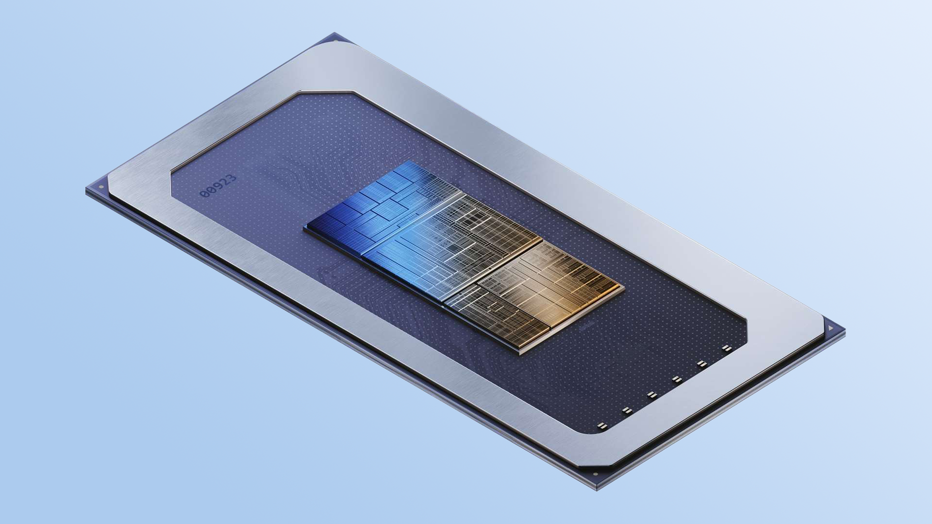
- Foveros 3D Chiplet Packaging
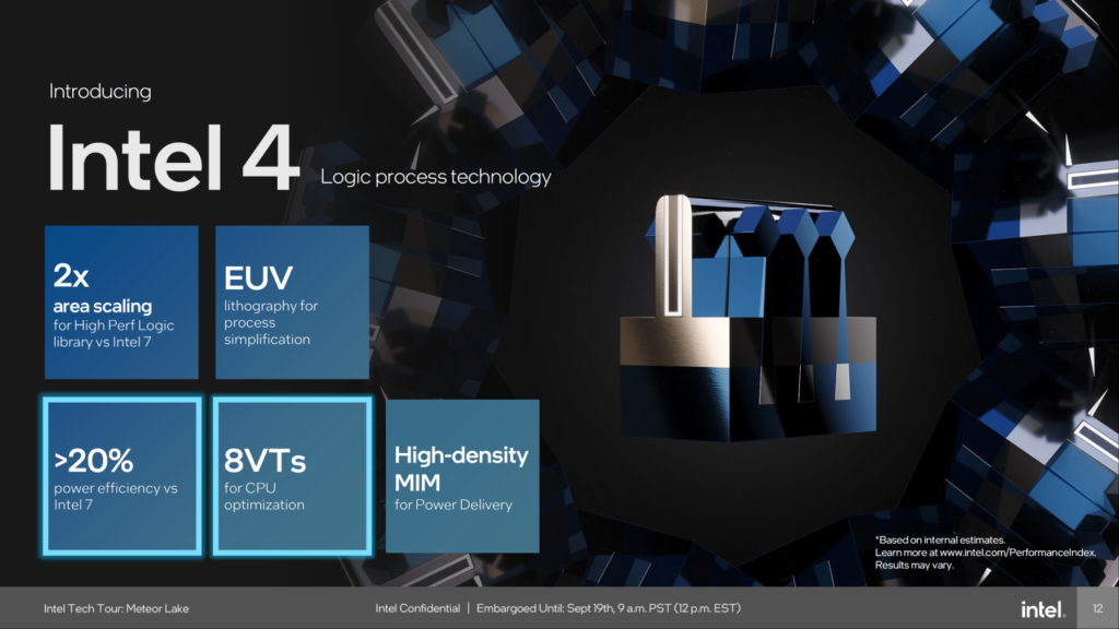
- Intel 4 Process with EUV (4nm Equivalent)
- Up to 14 Cores (6P+8E) for H/P Lineup | Up to 12 Cores (4P+8E) for U Lineup
- Intel Xe-LPG (Alchemist+) architecture for iGPU with 128 EUs
- Support for LPDDR5X-7467 and DDR5-5200 Memory
- PCIe Gen5, USB4, Thunderbolt 4
- VPU for AI Inference
- Triple Core Design (P-Cores, E-Cores, LPE-Cores)
- Intel’s First Consumer Disaggregated Design
- 3MB of L3 Cache per Slice/ 2MB of L2 Cache (P-Cores) | 4MB of L2 Cache (E-Core Cluster)
As you can probably see, Meteor Lake is no small ‘generational leap’. It can be taken as the baseline for Intel’s next decade with its new and innovative design.
– Intel 4 in All Its Glory
Meteor Lake uses the long-awaited ‘Intel 4’ node which is equivalent to TSMC’s N3 process, in terms of transistor density. However, we should point out that only the Compute Tile is manufactured on Intel 4. The rest of the CPU uses third-party nodes from TSMC.
– Foveros, The Era of 3D Packaging
Intel also boarded the chiplet hype train, introducing the industry’s first pure 3D design. AMD currently offers a 2.5D package with its CCD approach. The inclusion of X3D-Cache makes AMD’s V-Cache counterparts semi-3D or X-3D.
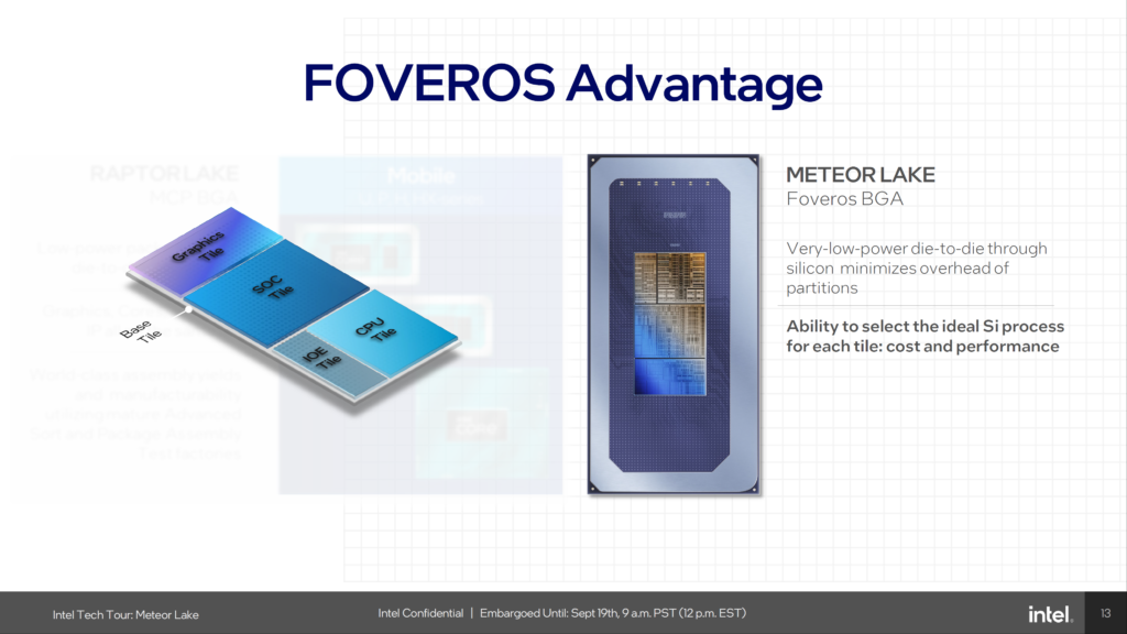
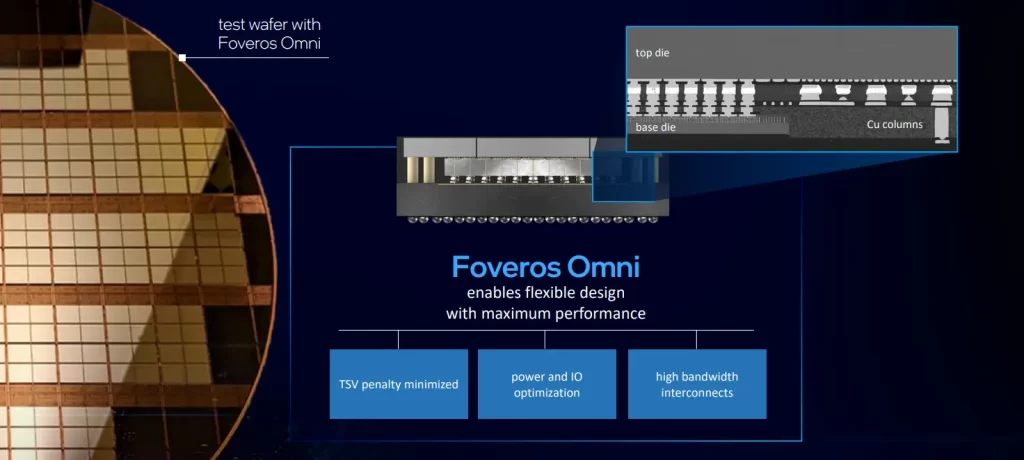
Meteor Lake uses Foveros Omni, 3rd Generation Foveros, with a 36-micrometer bump pitch. With Foveros Omni, Intel can stack top dies larger than the base die, such that the top die hangs from the edge. From these edges, Copper (columns) is used to deliver power, alleviating many of the limitations faced by TSVs.
Below is a small representation of how Foveros works with Meteor Lake. The ingredients to make a Meteor Lake CPU include: Compute Tile, I/O Tile, GPU Tile, and the SoC Tile. All these tiles are stacked on a Base Tile, which being active results in a 3D package.
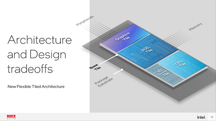
- Compute Tile: Intel 4
- SoC Tile: TSMC N6
- I/O Tile: TSMC N6
- Base Tile: Intel 22nm
- GPU Tile: TSMC 5N
– The Ingredients Behind Meteor Lake
Compute Tile: This tile is like AMD’s CCDs, hosting the physical cores, cache, and whatnot. The Compute Tile in Meteor Lake contains the Redwood Cove P-Cores and Crestmont E-Cores.
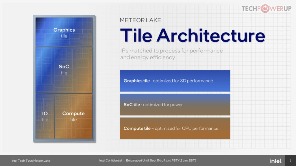
SoC Tile: The SoC Tile performs I/O functions similar to AMD’s IOD. Importantly, the SoC Tile integrates a VPU used for AI inference. This is Intel’s answer to Ryzen AI and will enable: Live Noise Suppression, Video Upscaling, Auto-Framing etcetera, offloading the burden from the CPU. It also packs the Media Accelerator, the Image Processing Engine and the Display Controller.
 SoC Tile Overview | Intel via Techpowerup

Inte incorporates an NOC (Network On Chip) to interconnect the various parts of the SoC Tile (See the second diagram). In the figure below, the SoC tile’s diversity is further proven by the fact that it functions as a PCH.
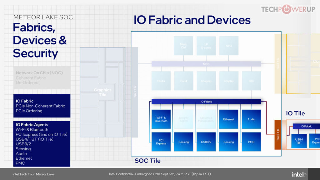
The SoC Tile is then connected via a Tile2Tile interface with the I/O Tile.
I/O Tile: The I/O Tile is actually better known as the IOE (I/O Extender) Tile. It hosts the USB4, Thunderbolt 4 interfaces and the PCIe physical layer. The inclusion of a separate I/O Tile is for scalability purposes. In reality, the I/O Tile is actually an extension of the already-versatile SoC Tile.

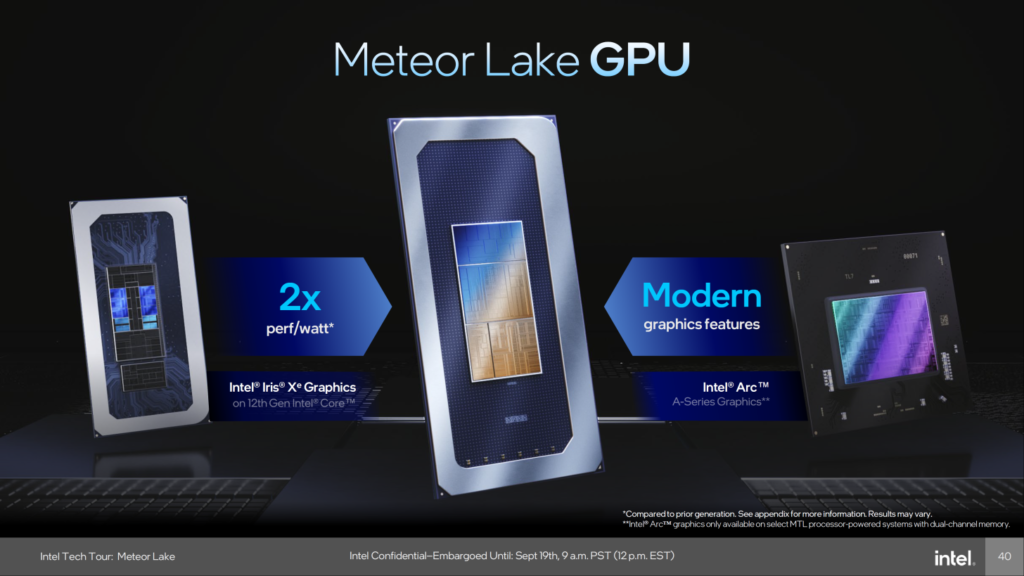
GPU Tile: The GPU Tile packs the iGPU for Meteor Lake. The iGPU is built using the Xe-LPG or Alchemist+ architecture. It can be considered something in between Alchemist and Battlemage.
– All the Xe-LPG Goodness
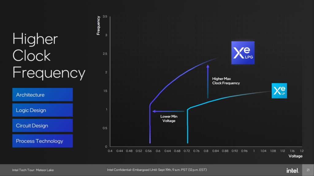
Meteor Lake will make use of Intel’s Xe-LPG architecture for its integrated GPU. Xe-LPG is a derivative of Alchemist, hence it inherits all the bells and whistles of Xe-HPG. A key feature of Meteor Lake’s iGPU is low-voltage operation and high-voltage for higher performance at the other end.
Basically, Meteor Lake’s iGPU can operate at powers as low as 10W. Moreover, users plugged-in the wall can enjoy high-refresh-rate gaming as Xe-LPG can boost remarkably high.
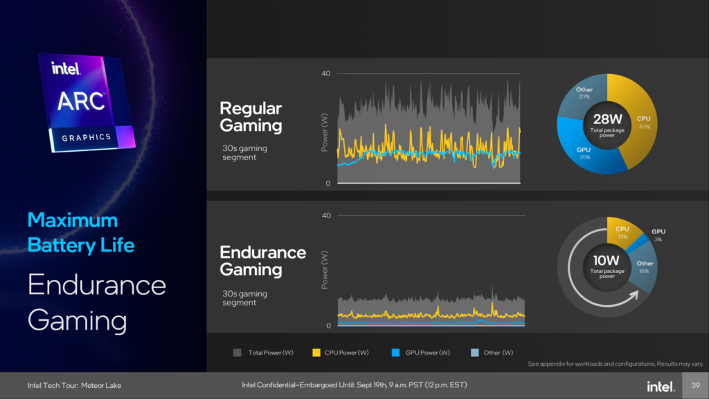
Xe-LPG can power your gaming needs at lower than 0.6V (600mV). That is insane since most GPUs do not operate under a voltage of 700mV, given the dangers of current leakage. This can drastically reduce power consumption, making Meteor Lake a great design choice for efficiency-centric laptops.
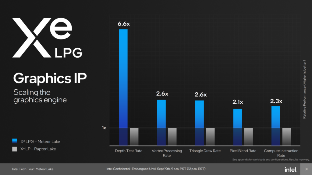
Enough with the chatter, more with actual numbers. Xe-LPG, powering Meteor Lake is 6.6x faster than RPL’s Xe-LP iGPU in the Depth Test Rate benchmark. More tests follow, seeing Xe-LPG always delivering more than two times than its predecessor.
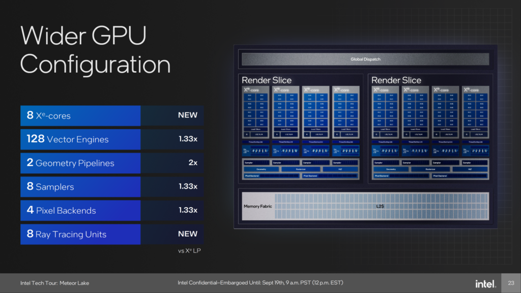
As Intel has adopted Alchemist as a base for Xe-LPG, it also packs the base Xe-Core unit, specifically tailored for laptops. We are to see a configuration of 8 Xe-Cores (128 EUs) and the introduction of Ray Tracing Units for the mobile segment.
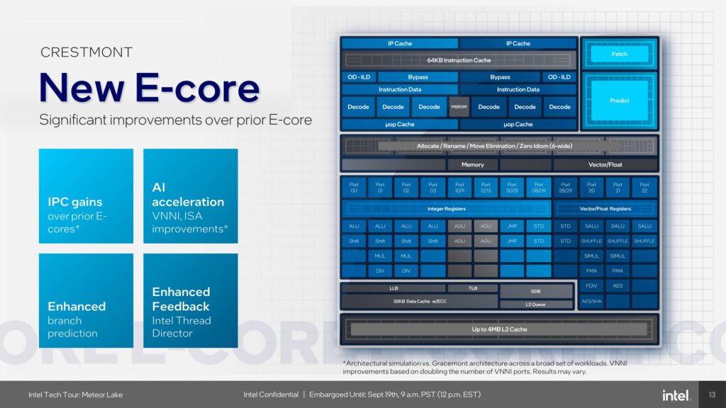
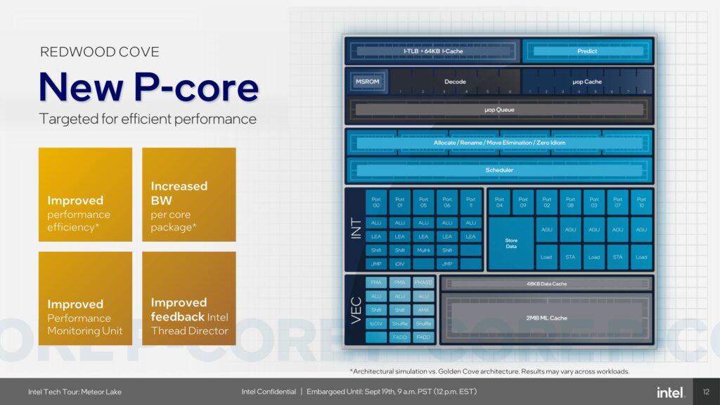
– Redwood Cove & Crestmont Cove µArchitecture
The new E-Core will be based on Crestmont, the successor to Gracemont present since Alder Lake. Intel promises ‘IPC Gains‘, ‘AI Acceleration‘, enhanced branch prediction and enhanced feedback.
Likewise, Redwood Cove has significant IPC gains over Raptor Cove. Intel reports that users should expect higher performance efficiency, higher bandwidth per core package and whatnot.
– AI For Everyone, Your Own NPU
Intel’s NPU, present in the SoC Tile is 8x more efficient in AI workloads than if you were to use a typical iGPU + CPU combination. The NPU will be available across all Meteor Lake SKUs.
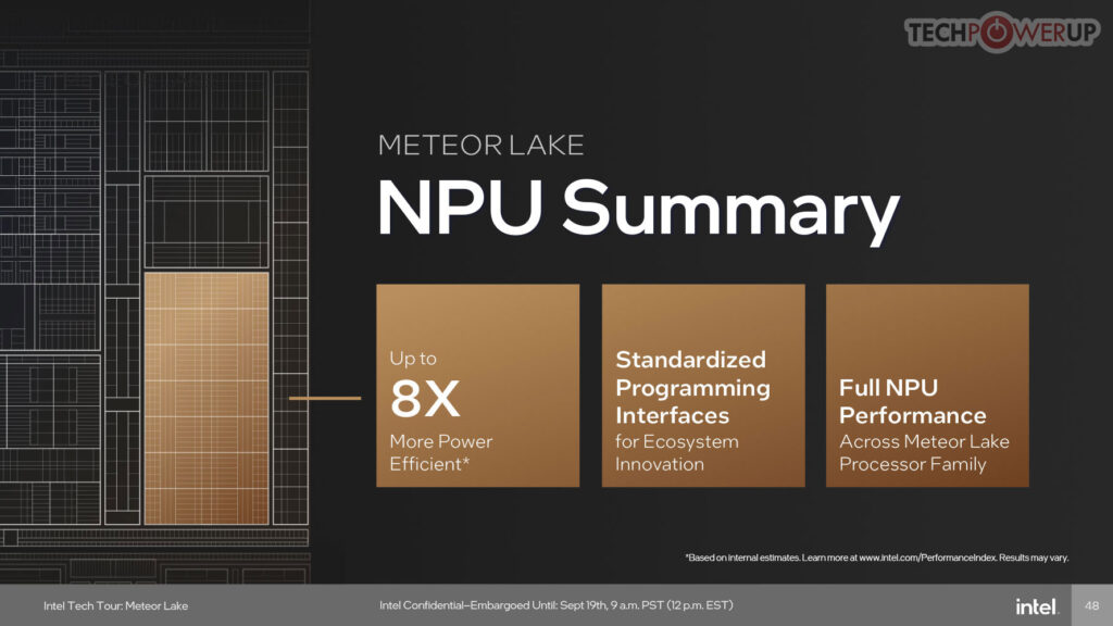
The NPU will come in handy for accelerating generative AI, LLMs, image, audio manipulation etcetera. Optimized software can use this NPU for AI-enabled super-resolution. Furthermore, it can prove to be beneficial while teleconferencing for noise suppression, auto framing and background removal/blur.
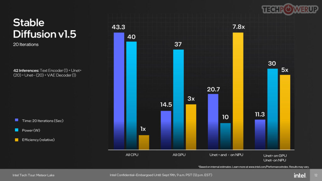
Without boring you with all the details and intricacies of the NPU, here’s a chart to show what Intel means. Keep a close eye at the yellow bars (efficiency).
The Meteor Lake Xe-LPG iGPU is 3x more efficient than the CPU, however, it doesn’t come close to the NPU, which is 7.8x more efficient. Simply put, the use of an NPU in suitable scenarios can grant you a 2x efficiency increase against your iGPU and a ~8x increase against your CPU.
Future Overview
Intel has confirmed the existence of Panther Lake, made using the 18A process node. Arrow Lake is almost ready and will make use of the 20A node, arriving next year. Panther Lake arrives 2025, and the design is so well-underway that Panther Lake will hit fabs by Q1 2024.

Furthermore, CEO of Intel, Pat Gelsinger held a 20A wafer in his hands, live at the Innovation Event. Pat remarked that the wafer is still warm, as it just came out of fab.
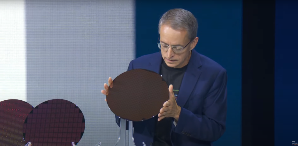
The CEO also showed off an Intel 3 wafer, which is used for the next-gen Granite Rapids Xeon processors. Intel touts a 2.4x efficiency gain over Sapphire Rapids. Granite Rapids is set to launch in 2024.
What’s more is that Pat didn’t stop at just Intel 3 and 20A. Intel 18A, scheduled for 2025 was also shown. Do note that this is just a test-chip and not a finalized product. However, Intel was very serious when it said it would push 5 nodes in 4 years.

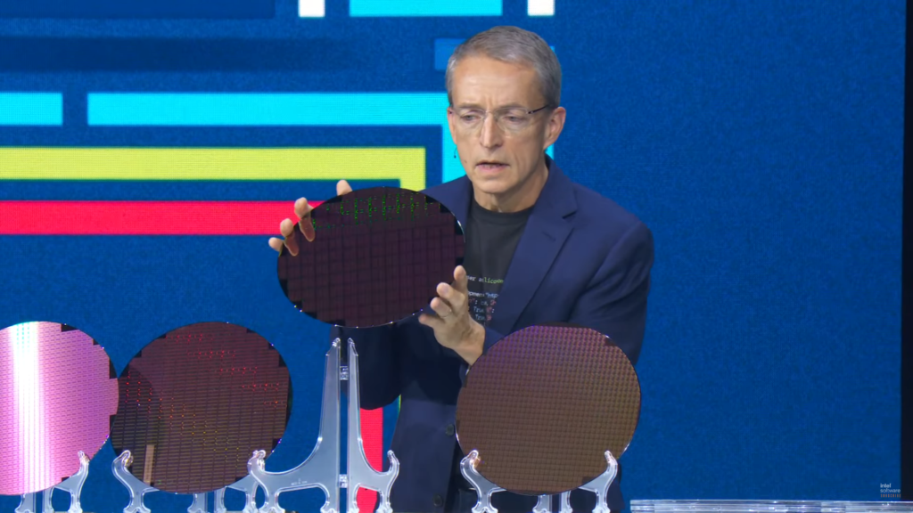
On the Xeon side of things, we already knew that Sierra Forest boasted a whopping 144 cores (Crestmont). But that was just one die. Fusing the two into a single package nets you 288 cores, and folks, that’s exactly what Intel is launching next year.
 Pat Gelsinger Showcasing a 288-Core Sierra Forest CPU

Read our article regarding the various wafers displayed at the Innovation Event here.
Summary
Meteor Lake is officialy out and is set to launch on the 14th of December. However, Intel did not show many benchmarks. The only comparions we saw were against Xe-LP. Moreover, there wasn’t a single display of the new cores in action.
What’s even more confusing is that Intel chose not to launch Raptor Lake Refresh today. The Innovation Event does span over a few days so keep an eye for something new at Intel Newsroom.