How To Make A HyperSensitive Intruder Alarm For Home?
Security alarms installed in homes are a big reason for decreased theft. Burglars enter the homes usually at night and when burglars enter the homes, firstly, they look for the security cameras and security alarms installed in the homes and then they move forward towards collecting the money and other valuable items. In this project, we will assemble an electronic circuit and then install it at a suitable place in the house. The preferred place is near to the light bulb which is installed on the top of the gate of the house and it is mostly turned ON at the night. When installing the circuit we will make sure that the circuit is placed near the light bulb because it comprises of an Infrared (IR) sensor and it detects any obstacle placed in front of it when it is placed in some brighter area.

How To Make A Domestic Intruder Alarm Using IR Sensor?
Now, as we have the basic idea of our project let’s move towards collecting the components, designing the circuit on software for testing and then finally assembling it on hardware.
Step 1: Components Needed (Hardware)
- No products found.
- LM358 (Operational Amplifier)
- No products found.
- No products found.
- No products found.
- No products found.
- No products found.
- No products found.
- No products found.
- 10k ohm Resistor
- 100 ohm Resistor
- No products found.
- PCB Board
- FeCl3
- Buzzer
- 12V Battery
- No products found.
- Soldering Iron
Step 2: Components Needed (Software)
- Proteus 8 Professional (Can be downloaded from Here)
After downloading the Proteus 8 Professional, design the circuit on it. We have included software simulations here so that it may be convenient for beginners to design the circuit and make appropriate connections on the hardware.
Step 3: Studying The Components
Now as we have made a list of all the components that we are going to use in this project. Let us move a step further and go through a brief study of all the main components.
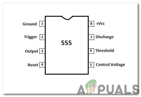
- 555 Timer IC: This IC has a variety of applications like providing time delays, as an oscillator, etc. There are three main configurations of the 555 timer IC. Astable multivibrator, monostable multivibrator, and bistable multivibrator. In this project, we will use it as an Astable multivibrator. In this mode, the IC acts as an oscillator that generates a square pulse. The frequency of the circuit can be adjusted by tuning the circuit. i.e. by varying the values of capacitors and resistors that are used in the circuit. The IC will generate a frequency when a high square pulse is applied to the RESET pin. We can achieve the output that we need by swapping the values of R4, R5 or by varying the value of the capacitor (C3). Pin 2 and pin 6 of the IC are shorted using a jumper wire to allow triggering after every cycle. In this project, the charging mechanism of Capacitor (C3) is that it charges through resistors (R4) and (R5) and it discharges through resistor Resistor (R5).
- LM-358 (Operational Amplifier): This IC consists of two high gain operational amplifiers and the unique thing about this IC is that a separate power source is not needed for the working of each comparator. Two inputs are inverting and non-inverting and there is one output. Furthermore, there are two pins Vcc and Ground. The inputs are V1 and V2. The input can be applied to either V1 or V2. V1 is a positive pin and is called a Non-inverting pin. V2 is the negative pin and is called the Inverting pin. The output from the amplifier is high when the non-inverting voltage (V1) is greater than the inverting voltage and the output is low when the inverting voltage (V2) is greater than the non-inverting voltage.

LM – 358 - IR Transmitter And Receiver Module: IR transmitter and receiver modules are widely used in electronic projects. For example, they are used in line tracking robots, domestic robots, etc. Both of them operate on 2 or 3 Volts and we drop the potential by connecting a resistor in series with the LED of IR transmitter. The transmitter radiates infrared signals. IR transmitter transmits any command and then the IR receiver which acts as a photodiode and senses that and responds accordingly. IR receiver works in reverse biased mode. A remote control patterns a glimpse of undetectable light which is transformed into instruction and is collected by the receiver module.

IR Transmitter And Receiver
Step 4: Working Principle Of The Circuit
The main role is of IR sensors in this project. Whenever an obstacle comes in front of an IR sensor, the rays that are transmitted by the transmitter are reflected towards the receiver. The potential is high at the output side of the Operational Amplifier when the rays are received by the IR receiver and in the circuit, the output is connected to the RESET pin of the 555 timer IC. The main role is of pin 4 of 555 timers because when the input voltage is low, the output voltage is also low and vice-versa. When we see the high output voltage a high-frequency signal is observed at the output side and we can make some modifications in the circuit to achieve this signal.
- Object Present: The circuit will be switched ON at night and whenever an obstacle is present in front of it the Receiver receives the Infrared radiations and output at the Op-Amp is high due to which Reset pin of 555 timer is high and the buzzer produces a loud sound.
- No Object Present: The circuit will remain switched OFF when no obstacle is present in front of it the Receiver doesn’t receive the Infrared radiations and output at the Op-Amp is low due to which Reset pin of 555 timer is low and the buzzer produces a no sound.
The output of the 555 timer IC is passed through a 1uF capacitor and then is fed to the buzzer which produces a loud and clear sound. The circuit will be placed at a suitable location in the house and it will be turned ON at night so, if any burglar tries to break-in, the alarm starts ringing and people inside the house call the Police after hearing the sound of the buzzer.

Step 5: Simulating the circuit
Before making the circuit it is better to simulate and examine all the readings on a software. The software we are going to use is the Proteus Design Suite. Proteus is a software on which electronic circuits are simulated.
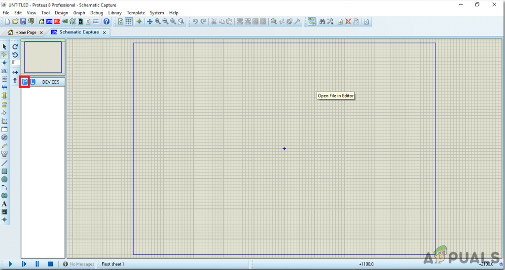
- After you download and install the Proteus software, open it. Open a new schematic by clicking the ISIS icon on the menu.

ISIS - When the new schematic appears, click on the P icon on the side menu. This will open a box in which you can select all the components that will be used.
New Schematic - Now type the name of the components that will be used to make the circuit. The component will appear in a list on the right side.

- In the same way, as above, search all the components. They will appear in the Devices List.

Component List
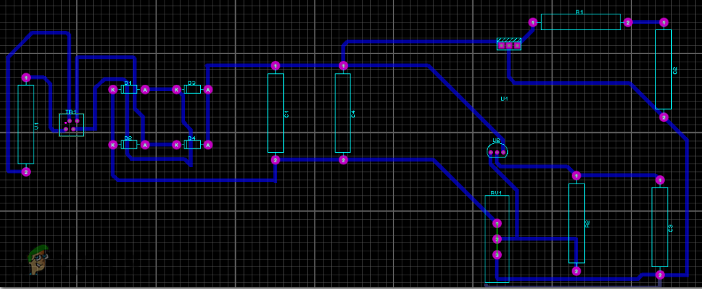
Step 6: Making a PCB Layout
As we are going to make the hardware circuit on a PCB, We need to make a PCB layout for this circuit first.
- To make the PCB layout on Proteus, we first need to assign the PCB packages to every component on the schematic. to assign packages, right mouse clicks on the component you want to assign the package and select Packaging Tool.
- Click on the ARIES option on the top menu to open a PCB schematic.
- From the Components List, Place all the components on the screen in a design you want your circuit to look like.
- Click on the track mode and connect all the pins that the software is telling you to connect by pointing an arrow.
- When the whole layout is made, it will look like this.
PCB Layout
Step 7: Circuit Diagram
After making the PCB layout the circuit diagram will look like this.

Step 8: Setting Up The Hardware
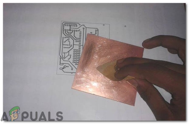
As we have now simulated the circuit on software and it is working perfectly fine. Now let us move ahead and place the components on PCB. A PCB is a printed circuit board. It is a board fully coated with copper on one side and fully insulating from the other side. Making the circuit on the PCB is comparatively a lengthy process. After the circuit is simulated on the software, and its PCB layout is made, the circuit layout is printed on a butter paper. Before placing the butter paper on the PCB board use the PCB scrapper to rub the board so that the copper layer on board is diminished from top of the board.
Then the butter paper is placed on the PCB board and ironed until the circuit is printed on the board (It takes approximately five minutes).

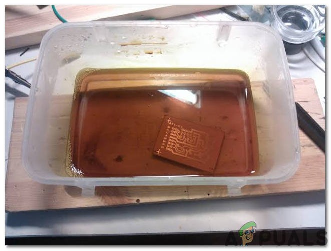
Now, when the circuit is printed on the board, it is dipped into the FeCl3 solution of hot water to remove extra copper from the board, only the copper under the printed circuit will be left behind.
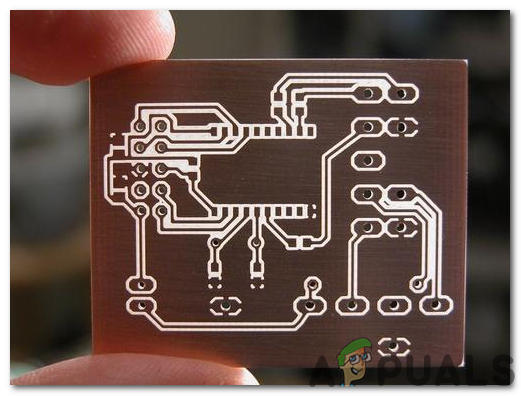
After that rub the PCB board with the scrapper so the wiring will be prominent. Now drill the holes in the respective places and place the components on the circuit board.
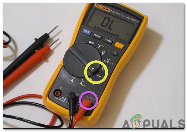
Solder the components on the board. Finally, check the continuity of the circuit and if discontinuity occurs at any place de-solder the components and connect them again. It is better to apply hot glue using a hot glue gun on the positive and negative terminals of battery so that the terminals of battery may not be detached from the circuit.
Place the hardware at a suitable place near the door and it is switched ON at night and switched OFF in the morning. The preferred location is near to the gate of the house so that if any robber tries to enter the house at night the alarm starts ringing and neighbors or security guards come to know that the people living in the house need help.


