The Zen4 ‘Raphael’ I/O Die Has Been Mapped Out
User lixnjen on Twitter obtained a screenshot of the I/O die featured on AMD’s Zen4 CPUs. While the die-shot itself is not self-explanatory, another user namely ‘Locuza‘ took the time to label the diagram.
This is probably the first I/O shot of the 6 nm-based I/O (Zen4 IOD) die used for AMD’s Raphael or Ryzen 7000 lineup of CPUs. The HEDT platform, on the other hand, features another I/O die given the higher specs.
The reference image has been taken from AMD’s slides at ISSCC 2023. AMD at that event, revealed its plans for Zettascale (1000x more than Exascale) computing. More on that here. The diagram below explains how AMD has designed the I/O die for the Ryzen 7000 class of consumer CPUs.
On the very left, we can see the 160b (2x 2×40) DDR5 PHY, which is divided into 128b for DDR5 PHY and 32b for ECC. On the top exist the GMI3 ports which connect the I/O die or chiplet to the main Zen4 CCD. Locuza mentions that this configuration (2xGMI3) would not allow for more than 2 CCDs (16 cores) on any Raphael product.
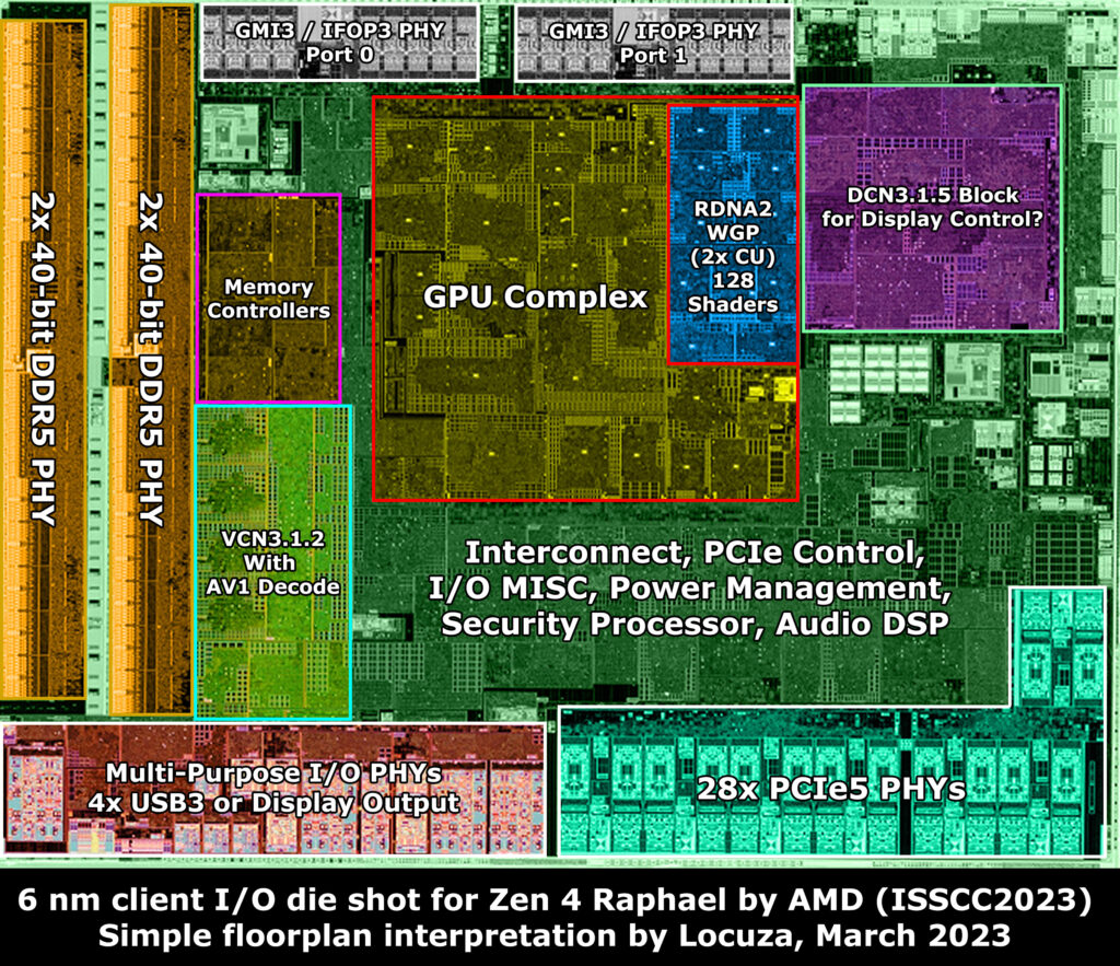
The PCIe Gen 5.0 lanes are present at the bottom right and are 28 to be exact. That is a decrease from previous generations, which had upwards of 32 lanes (such as the 5950X). At the heart of the I/O die exists the GPU Complex housing the RDNA2 iGPU boasting 128 shading units (2 CUs). Apparently, there is no native USB4 support in the Zen4 IOD.
Below the memory controllers lie the VCN 3.1.2 video encoding/decoding hardware accelerators. For context, VCN 3.1.2 brings fort AV1 decode support. However, AV1 encoding is a feature exclusive to RDNA3 for now.