Intel Entirely Restructures its Foundry Division
We all have been aware of Intel’s problems for the past few years. When push came to shove, the giant was taken aback by how quick competitors were to catch up. The problem for Intel is that it’s not just a chip manufacturer, but also has an entire fabrication division to look after. IFS or Intel Foundry Services will undergo various changes, enabling Intel to catch up to the rest of the market.
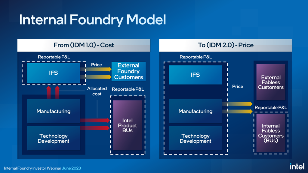
The initial success of Intel’s IDM 1.0 (Integrated Design Manufacturer) approach was long-lasting but sadly ended. Intel is effectively an IDM since it designs and manufactures its own chips instead of relying on other fabs.

Making matters worse, the 10nm delay was probably the final nail in the coffin for Intel. AMD was in a much better position due to a smaller transistor size thanks to TSMC. Intel lagged severely with its 10th-generation and 11th-generation offerings, where reviewers perceived these processors as a waste of sand.
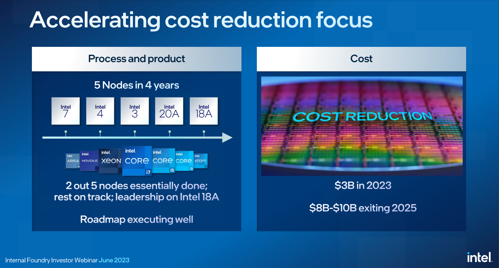
We are past that point, however, the game is not yet over. Intel is again, one step behind of the competition and could very well be behind for a few more years. You can probably see the importance of Intel 20A and Intel 18A as these nodes are make-it-or-break-it for Intel.
In light of these problems, the company has taken various steps to reclaim its once-acclaimed position. The headline today is that Intel is now opting for an internal foundry model. Let’s explain how that works.
The Internal Foundry Model
In very simple terms, an internal foundry model basically states that Intel’s own business units will engage or deal with Intel’s fabrication unit in the same way as third-party sources. Intel calls this model ‘IDM 2.0‘, or the next step-up from IDM 1.0.
Seeing how Intel has both CPU design and silicon manufacturing units, it is no secret that this CPU design unit had better access and greater advantages than an external buyer, say NVIDIA.
We haven’t seen Intel design any of NVIDIA’s chips, yet, but this was just an example. This model has many different constituents, however, it boils down to the following benefits:
- Reducing costs by $3 Billion by 2023
- Reducing costs by $8–10 Billion by 2025
- Achieving non-GAAP gross margins of 60%
- Achieving operating margins of 40%
- Becoming the second largest foundry by next year
- Attaining manufacturing revenue higher than $20 Billion.
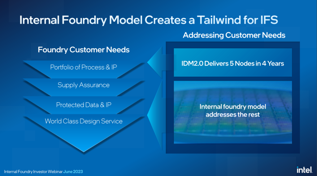
A key factor to regaining Intel its top-dog spot is smaller and better process nodes. Team Blue now plans to be more aggressive than ever in an attempt to catch up to TSMC. Intel 4 will take off later this year, with Intel 20A and 18A arriving shortly.
In 2025, Intel plans to have at least 5 different products based on this 18A process. The ramp up will initiate at an internal level, ironing out all the problems before Intel presents this cutting-edge node to external IFS customers.
The second factor is this new scheme for its foundry services, where Intel will treat business units similarly to external consumers. The advantages and important elements of this strategy have been discussed below.
Advantages
Following are a few advantages offered by the IDM 2.0 scheme:
-A Sense of Accountability
With this new model, Intel’s manufacturing groups will be held accountable to P&L or profit and loss for the first time. Furthermore, it will achieve a balance between external and internal consumers by offering them similar market-driven rates, assuring certainty and stability.
What’s better is that the internal divisions will have to compete for silicon volume much like third-party customers. This will cause external customers to prefer Intel over its competitors and also drive the internal units to meet the required criteria without exhausting precious foundry resources.
-Expedited Wafers
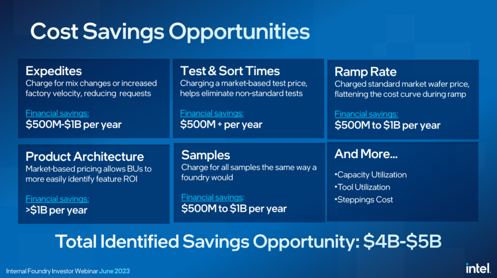
Another advantage of this strategy is that the business units will now bear the cost of expedited wafers.
In semiconductor manufacturing, a batch of wafers can sometimes be given a high-priority status due to many reasons. These wafers are rushed and vital resources are spent on processing this specific batch. An example can be to test industry-first process nodes such as 3nm. Intel will prefer to process these wafers faster than others, simply to beat the competition.
Simplified Definition of an Expedited Wafer
Generally, Intel used to spend a lot of time and effort processing these batches, providing a sort of subsidy to the business units. However, as external customers for Intel will continue to increase, the internal units will have to pay for this service.
This process is typically inefficient but can result in quicker processing of wafers. All companies like to achieve an equilibrium between time and efficiency. Intel seems to be following the same model.
This small change alone can save Intel $500 Million – $1 Billion annually.
-Time Penalty
Intel’s business units require 2-3x longer test times as compared to its competitors. This leads to inefficiency and delays, if things go south.
From now on, internal units will be charged market prices based on their test times. This will make these divisions more conscious of their decisions and will drive innovation. Due to this penalty, Intel can enjoy savings of $500 Million annually.
Another problem that Intel faces is that it develops too many SKUs or different versions derived from a base design. This is primarily done to diversify your offerings for more segments.
Long story short, Intel develops too many chips and has more than one base design for the same market. This is a huge disadvantage in contrast to the likes of AMD which uses same dies for both server and mainstream markets, whenever possible.
Moreover, we will see a reduced number of steppings by Intel in the near future. Steppings are same physical copies of the same product, with additional improvements. By utilizing its resources and expenditure carefully, Intel can save $500 Million – $1 Billion.
The Takeaway
IDM 2.0 is a crucial stage for Intel, reassuring the trust of investors in the company. The model is quite simple to understand but is really effective and essential for Intel to achieve its goals.
Chipzilla will construct a clear wall between its BUs and the IFS, but that in itself is an advantage for Intel. Due to the lack of subsidized services, the BUs will have to be efficient and their plans must be cost-effective. On the other hand, external partners such as AMD and NVIDIA may opt for Intel in the near future, if TSMC or other manufacturers fail to provide high-quality wafers.
Source: Intel