Huawei Patent Reveals New Cost-Effective Method of Semiconductor Packaging
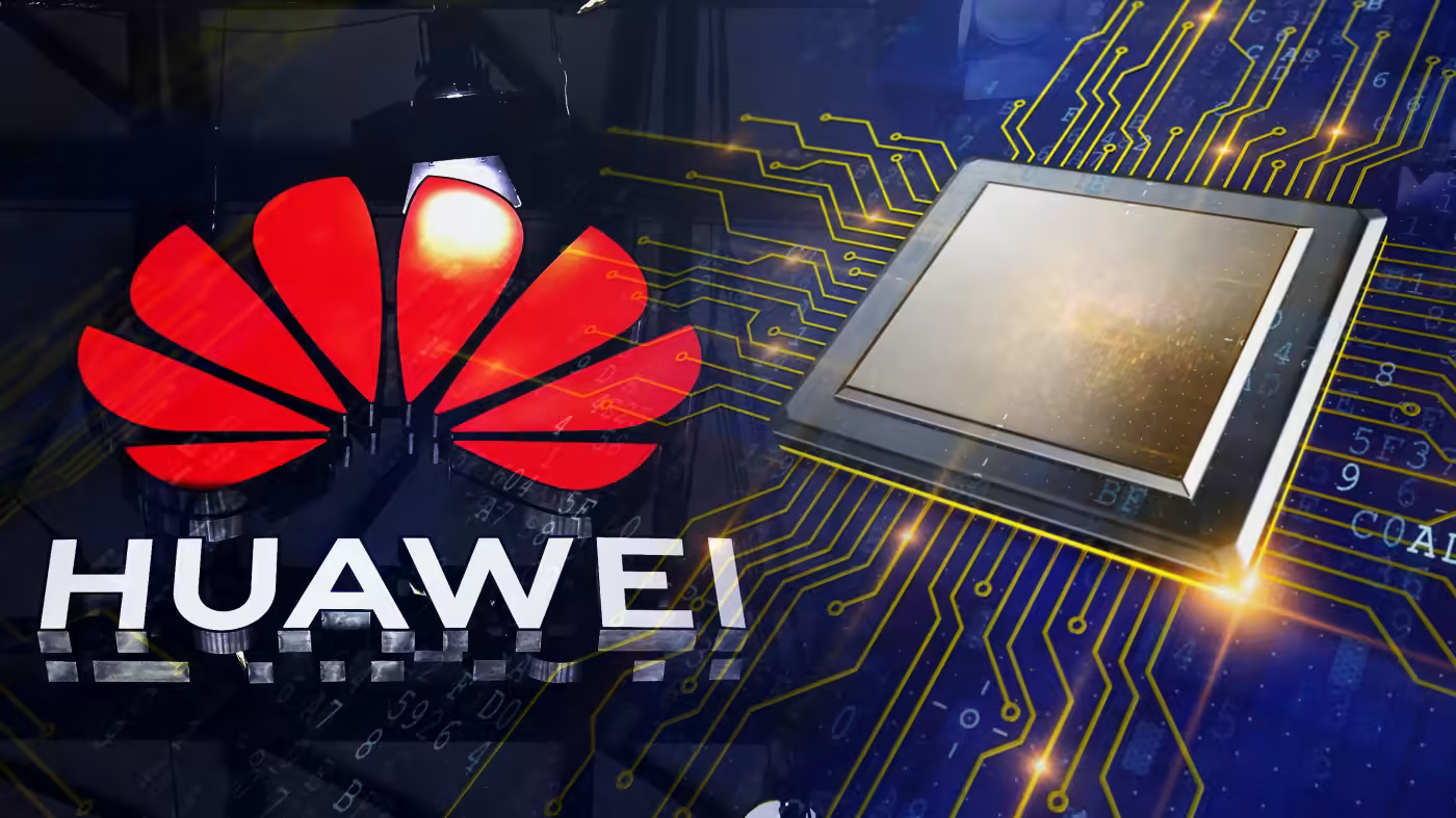
A new Huawei patent on chipset packaging technique that might lower total production cost of the semiconductor was recently released by the Chinese Patent Department. These patents are newest additions that emerged in tandem with Huawei’s efforts to perfect the chipset production process.
From what we can see, Huawei has a patent application named “semiconductor packaging” (CN116097432A) in the works. The application for this invention was filed on September 8, 2021, and it was approved and published on May 9, 2023.
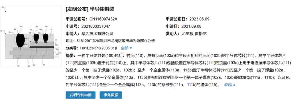
A semiconductor chip (111) with a top surface (103a) and a bottom surface (103b) opposite the top surface are included in a semiconductor package (100), with the bottom surface of the semiconductor chip (111) (103b) positioned on the substrate (110).
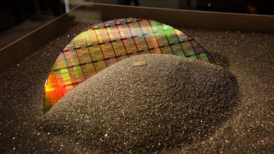
A semiconductor package is a container for one or more semiconductor devices or integrated circuits that may be made of metal, plastic, glass, or ceramic. Semiconductor wafers (often silicon) are used to create individual components, which are then sliced into the die, tested, and packaged. Leads like lands, balls, or pins allow the package to be connected to an external environment like a printed circuit board.
This technology allegedly lowers production costs and offers an alternate mold embedding method. It also allows for the dependable and productive production of semiconductor packages.
Huawei’s latest chipset packaging technology patent demonstrates the company’s dedication to improving semiconductor production.
Source: Huawei Central