How To Design FM Bugger Circuit?
The bugger is a device that is used for finding out the location of someone. It finds out the location of a person and then tells that location to someone who is asking for. A status of a person is known if we have this circuit installed at our homes or offices. This circuit can be considered illegal but most of the secret agencies use it to track the location of someone. After assembling this circuit a normal FM radio set will be needed to listen to the conversation between two people over a long distance. This circuit would be placed at the desired location for listening to the conversation between two people. The circuit that is explained as under will be placed at the transmitter side and at the receiver’s side Normal FM radio would be needed to hear that transmitted voice but one thing that needs to be under consideration is that the frequency at the receiver’s end must be tuned to the frequency of the transmitter.
How To Integrate Basic Electronic Components In Assembling The Circuit?
The best approach to start any project is to make a list of components and going through a brief study of these components because no one will want to stick in the middle of a project just because of a missing component. The Printed Circuit Board is preferred for assembling the circuit on hardware because if we assemble the components on breadboard they may detach from it and the circuit will become short hence, PCB is preferred.
Step 1: Components Used (Hardware)
- 2N2222 Transistor
- Copper Wire
- 22k Ohm Resistor
- 47k Ohm Resistor
- No products found.
- 1nF Capacitor (x3)
- No products found.
- No products found.
- No products found.
- Tacticle Switch
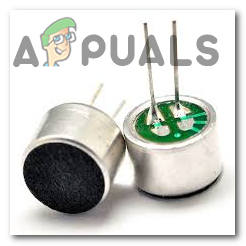
- Condenser Microphone Electret
- 9V Battery
- No products found.
- FeCl3
- No products found.
- Printed Circuit Board
- Hot Glue Gun
Step 2: Components Used (Software)
- Proteus 8 Professional (Can be downloaded from Here)
After downloading the Proteus 8 Professional, design the circuit on it. I have included software simulations here so that it may be convenient for beginners to design the circuit and make appropriate connections on the hardware.
Step 3: Studying The Components
As we now know the main idea behind the project, and we also have a complete list of all the components, let us move one step ahead and go through a brief study of all the components.
Electret Microphone: An Electret Microphone is a capacitor-based microphone. By using this microphone, the need for polarizing power supply is eliminated by using a permanently charged material, used to convert sound into an electrical signal. An electret is a ferroelectric material that has been for all time electrically charged or energized. Because of the high obstruction and substance steadiness of the material, the electrical charge won’t rot for many years. The name originates from “electrostatic and magnet”; a static charge is inserted in an electret by the arrangement of the static charges in the material, much how a magnet is made by adjusting the attractive spaces in a bit of iron. These Mics are widely used in GPS systems, hearing aids, telephones, voice over IP, Speech recognition, FRS Radios, etc.
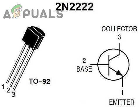
2N2222 Transistor: It is the most renown NPN bipolar junction transistor. This transistor is mostly used for switching and amplification purposes. The main reason behind its fame is that it is low cost, small size and its ability to handle a high value of current as compared to the similar small transistors. Normally this transistor can handle a high current rating up to 800mA. This transistor is made up of silicon or germanium material. In the process of amplification, the input analog signal is applied to its collector and the output amplified signal is sent to the base. this analog signal could be a voice signal.
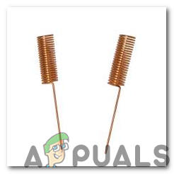
Copper Wire Antenna: Instead of buying an antenna it could be designed at home. For designing the antenna a copper wire is needed. It is a very easy task and after designing the copper wire antenna we could improve radio reception over a variety of frequency ranges. For designing the copper wire antenna at your home click Here
Step 4: Block Diagram
The block diagram of the circuit is shown below for analyzing the overall project working:
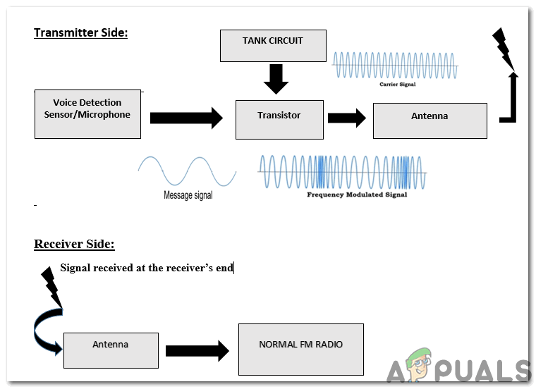
Step 5: Interpretation Of The Block Diagram
At the transmitter side, the Modulation technique is used. The message signal is transmitted with the high-frequency carrier signal over a channel. The carrier signal is generated by the tank circuit. The transistor acts as a modulation device here and after modulation, it transmits the signal in the air with the help of an antenna. This modulated signal is received at the receiver’s end by the antenna and it is fed to the FM Radio. Then at the receiver’s end, the user can listen to the conversation going on. The person at the receiver’s end would set the receiver’s frequency on the radio so that he/she may be able to hear the voice.
Step 6: Working Of The Circuit
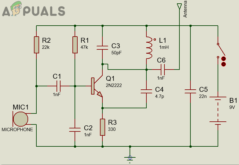
There are three types of modulation techniques named as amplitude modulation, frequency modulation, and phase modulation. In this project, we will use the frequency modulation technique on the transmitter side. The frequency of the carrier wave is altered. In this circuit, the message signal is generated by the transmitter and a high-frequency carrier signal is superimposed on that message signal. The Frequency modulation is preferred over amplitude modulation because the amplitude of Frequency modulated wave remains constant over time. In amplitude modulation, the noise is added over the channel hence, the transmitted message is distorted. The microphone placed at the transmitter side will decode the message into a signal. The capacitor (C1) will remove that noise and then it will pass on the signal to the transistor. In this circuit, the tank circuit is made up of the capacitor C6 and inductor L1. The transistor will work as an amplifier and it will amplify both carrier and message signal and send it to the air through the antenna. The capacitor C4 is placed in the circuit before the antenna to remove the noise from the transmitted signal. The carrier signal must be in the range of 88 to 105 MHz so that the FM radio receiver can receive your transmitted signal. The FM Radio set will be adjusted at a specific frequency for listening to the conversation.
Step 7: Simulating the circuit
Before making the circuit it is better to simulate and examine all the readings on a software. The software we are going to use is the Proteus Design Suite. Proteus is a software on which electronic circuits are simulated:
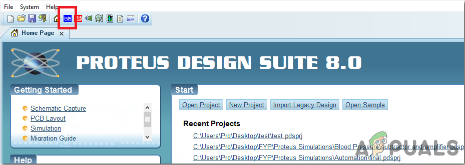
- After you download and install the Proteus software, open it. Open a new schematic by clicking the ISIS icon on the menu.
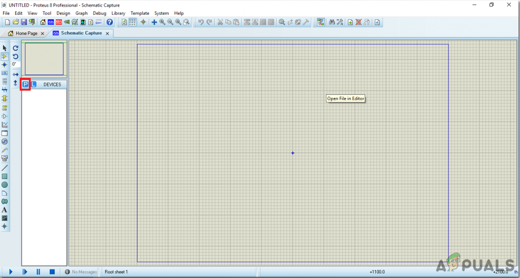
ISIS - When the new schematic appears, click on the P icon on the side menu. This will open a box in which you can select all the components that will be used.
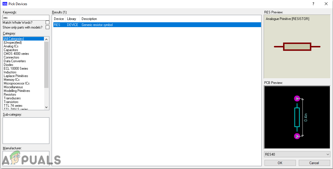
New Schematic - Now type the name of the components that will be used to make the circuit. The component will appear in a list on the right side.
Selecting Components - In the same way, as above, search all the components. They will appear in the Devices List.
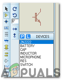
Components List
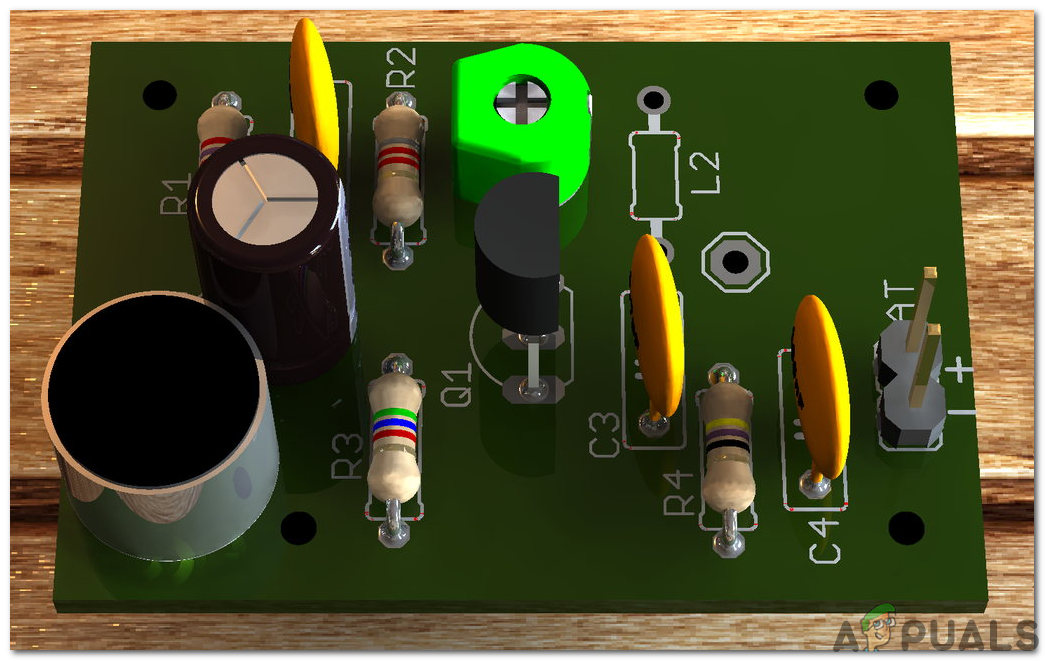
Step 8: Circuit Diagram
After assembling the components and wiring them, the circuit diagram should look like this:
Step 9: Making a PCB Layout
As we are going to make the hardware circuit on a PCB, We need to make a PCB layout for this circuit first.
- To make the PCB layout on Proteus, we first need to assign the PCB packages to every component on the schematic. to assign packages, right mouse clicks on the component you want to assign the package and select Packaging Tool.
- Click on the ARIES option on the top menu to open a PCB schematic.
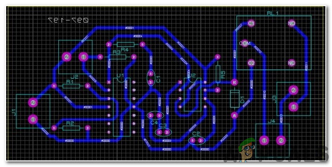
ARIES Design - From the Components List, Place all the components on the screen in a design you want your circuit to look like.
- Click on the track mode and connect all the pins that the software is telling you to connect by pointing an arrow.
Step 10: Assembling The Hardware
As we have now simulated the circuit on software and it is working perfectly fine. Now let us move ahead and place the components on PCB. A PCB is a printed circuit board. It is a board fully coated with copper on one side and fully insulating from the other side. Making the circuit on the PCB is comparatively a lengthy process. After the circuit is simulated on the software, and its PCB layout is made, the circuit layout is printed on a butter paper. Before placing the butter paper on the PCB board use a scrapper to rub the board so that the copper layer on board is diminished from top of the board.
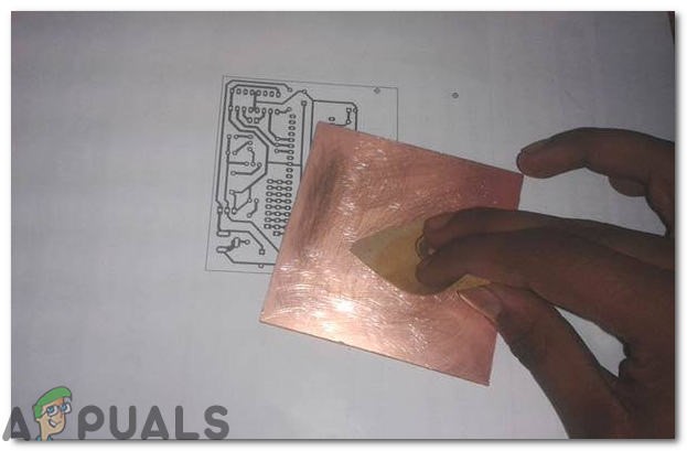
Then the butter paper is placed on the PCB board and ironed until the circuit is printed on the board (It takes approximately five minutes).

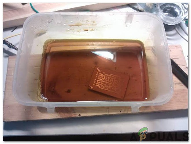
Now, when the circuit is printed on the board, it is dipped into the FeCl3 solution of hot water to remove extra copper from the board, only the copper under the printed circuit will be left behind.
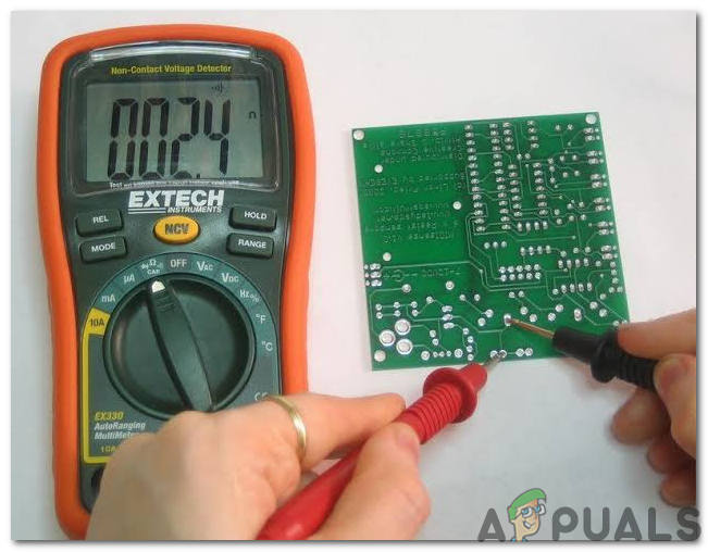
After that rub the PCB board with the scrapper so the wiring will be prominent. Now drill the holes in the respective places and place the components on the circuit board.

Solder the components on the board. Finally, check the continuity of the circuit and if discontinuity occurs at any place de-solder the components and connect them again. Apply hot glue gun on the circuit terminals so the battery may not be detached if any pressure is applied.
Step 11: Testing The Circuit
Now, our hardware is fully ready. Place the circuit in the room to listen to the conversation between two people. Turn ON the battery to test the circuit. Continuously monitor the battery and replace the battery when it dries out